
1
Date: 05/25/04 SPX2931 100mA Low Dropout Voltage Regulator
© Copyright 2004 Sipex Corporation
100mA Low Dropout Voltage Regulator
SPX2931
DESCRIPTION
FEATURES
3.3V and 3.5V Versions
Output Current in Excess of 100 mA
Input-Output Differential is 0.3 at 100mA
Mirror-Image Insertion Protection
Internal Thermal Protection
Available in TO-92 and SOT-89 Packages
Improved Version of the Industry
Standard LM2931
Reverse Battery, Internal Short Circuit,
20V Reverse Transient and 60V Load
Dump Protection
Availiable with either 2% or 3% Output
Accurancy at 25∞C
Æ
The SPX2931 is a low power, positive voltage regulator. This device is an excellent choice for
use in battery-powered applications such as cordless telephones, radio control systems, and
portable computers. The SPX2931 features offers very low quiescent currents (0.4 mA), and very
low drop output voltage (50 mV at light load and 300 mV at 100 mA). The SPX2931 is offered
in a 3-pin TO-92, and SOT-89 package.
APPLICATIONS
Portable Instrumentation
Cordless Telephones
Radio Control Systems
TYPICAL APPLICATIONS CIRCUIT
Now Available in Lead Free Packaging
SPX2931
V
IN
C
1
V
OUT
1µF
100µF,
ESR 0.05 to 0.6
ohms
Gnd
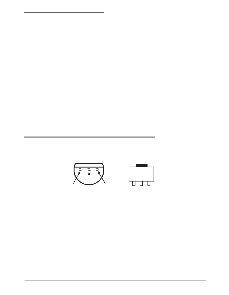
Bottom View
TO-92 (N)
SOT-89 (M1)
Top View
1
2
3
V
IN
GND
V
OUT
1
3
2
GND
V
IN
V
OUT

2
Date: 05/25/04 SPX2931 100mA Low Dropout Voltage Regulator
© Copyright 2004 Sipex Corporation
PARAMETER
CONDITIONS
MIN
TYP
MAX
MIN
TYP
MAX
UNITS
3.3V Version
Output Voltage (Note 2) 4V < V
IN
<26V,
3.234
3.300
3.366
3.201
3.300 3.399
I
O
= 100 mA over temp.
V
3.201
3.300
3.399
3.135
3.300 3.465
3.5V Version
Output Voltage (Note 2) 4.5V < V
IN
< 26V,
3.430
3.500
3.570
3.395
3.500 3.605
I
O
= 100mA Over Temp.
V
3.395
3.500
3.605
3.325
3.500 3.675
All Voltage Options
Long Term Stability
20
20
mV/1000hr
Line Regulation
9V<V
IN
<16V,
2.0
10
4.0
30
mV
4.5V<V
IN<
26V
4.0
30
Load Regulation
5mA<I
O
< 150mA
14
50
14
50
mV
Dropout Voltage
I
O
=10mA
0.05
0.2
0.05
0.2
I
O
=150mA
0.3
0.6
0.3
0.6
V
Quiescent Current
I
O
=10mA, 4.5V<V
IN
<26V
0.4
1.0
0.4
1.0
-40∞C<Tj<85∞C
15
15
mA
I
O
=150mA, VI
N
=14V,
T
J
=25∞C
Output Noise Voltage
10Hz-100kHz, C
OUT
=100µF
500
500
µV
RMS
Ripple Rejection
F
O
=120Hz
80
80
dB
Maximum Operational
Input Voltage
26
26
V
Maximum Line Transient R
L
= 500, 100ms
60
70
50
70
V
Reverse Polarity Input
V
O
> -0.3V, R
L
= 500
-15
-30
-15
-30
V
Voltage, DC
Reverse Polarity Input
1% Duty Cycle, <100ms
-50
-80
-50
-80
V
Voltage, Transient
R
L
=500
ABSOLUTE MAXIMUM RATINGS
Power Dissipation (note 3) ........................................ Internally limited
Lead Temp (soldering, 5 seconds) ............................................ 260∞C
Storage Temperature Range ..................................... -65∞C to +150∞C
Input Supply Voltage Range ............................................. -0.3 to +30V
ESD Rating (note 4) ...................................................................... 2kV
NOTES:
Note 1: See TYPICAL APLICATIONS notes to ensure constant junction temperature, low duty cycle pulse testing used.
Note 2: All limits are at 25
∞C or over the full operationg junction temperature range of -40∞C to +125∞C.
Note 3: The maximum power dissipation is a function of maximum junction temperature, total thermal resistance, and ambient temperature.
Note 4: Human body model, 100pF discharged through 1.5k
.
at V
IN
=6V, T
A
= 25∞C, I
O
= 10 mA, C
OUT
= 100 µF, unless otherwise specified. (Note 1)
RECOMMENDED OPERATING CONSITIONS
Input Voltage Range ........................................................... 3.0 to 26V
Operating Junction Temperature Range ..................... -40∞C to 125∞C
TO-92
JA
............................................................................... 160∞C/W
SOT-89
JA
............................................................................ 110∞C/W
ELECTRICAL CHARACTERISTICS

3
Date: 05/25/04 SPX2931 100mA Low Dropout Voltage Regulator
© Copyright 2004 Sipex Corporation
Figure 1. Quiescent Current
Figure 2. Quiescent Current
Figure 3. Dropout Voltage
Figure 4. Dropout Voltage
Figure 5. Peak Output Current
Figure 6. Low Voltage Behavior
25
6
4
0
-40
0
80
120
JUNCTION TEMPERATURE (∞C)
QUIESCENT CURRENT (mA)
10
15
20
2
~
~
~
~
40
I
O
= 0mA
I
O
= 50mA
I
O
= 100mA
QUIESCENT CURRENT (mA)
0
0
OUTPUT CURRENT (mA)
30
60
90
5
10
15
20
25
30
V
IN
= 14V
INPUT OUTPUT DIFFERENTIAL (V)
0.6
0.5
0.2
0
JUNCTION TEMPERATURE (∫C)
0.4
0.3
0.1
0
40
80
120
I
O
= 100mA
I
O
= 50mA
I
O
= 10mA
INPUT OUTPUT DIFFERENTIAL (V)
0.4
0.2
OUTPUT CURRENT (mA)
0.3
0.1
0
0
50
100
0.5
0.6
OUTPUT CURRENT (mA)
800
500
0
INPUT VOLTAGE (V)
200
100
10
20
300
400
30
0
T
J
= 25∫C
T
J
= 85∫C
T
J
= -40∫C
6.0
3.0
2.0
1.0
2.0
3.0
4.0
5.0
6.0
INPUT VOLTAGE (V)
OUTPUT VOL
T
AGE (V)
4.0
5.0
SPX2931 3.5
I
O
= 100 mA
TYPICAL PERFORMANCE CHARACTERISTICS

4
Date: 05/25/04 SPX2931 100mA Low Dropout Voltage Regulator
© Copyright 2004 Sipex Corporation
Figure 7. Maximum Power Dissipation (SOT89)
Figure 8. Maximum Power Dissipation (TO-92)
Figure 9. Output Impedance
Figure 10. Operation During Load Dump
APPLICATION INFORMATION
The SPX2931 requires an output capacitor for
device stability. The value required varies greatly
depending upon the application circuit and other
factors. The high frequency characteristics of
electrolytic capacitors depend greatly on the
type and also on the manufacturer. Sometimes
bench testing is the only means to determine the
proper capacitor type and value. The high qual-
ity 100
∞F aluminum electrolytic covers all gen-
eral application circuits, this stability can be
obtained with a tantalum electrolytic value of
47
∞F.
Another critical point of electrolytic character-
istics is its performance over temperature. The
SPX2931 is designed to operate starting at -
40
∞C which may not be true in the case of
electrolytic. Higher temperatures generally no
problem. The electrolytic. type in aluminum
will freeze around -30
∞C. This could cause an
oscillation at output of regulator. At a lower
temperature requirement by many applications
the capacitor should maintain its performance.
So as a result, for an application which regulator
junction temperature does not exceed 25
∞C, the
output capacitor can be reduced by the factor of
two over the value needed for the entire tem-
perature range.
0.0
0 10 20
40
70 80
AMBIENT TEMPERATURE (∫C)
POWER DISSIP
A
TION (W)
30
50 60
90
0.4
0.8
1.2
1.6
2.0
1.0
0
20
40 50 60
AMBIENT TEMPERATURE (∫C)
POWER DISSIP
A
TION (W)
0.9
0.8
0.7
0.6
0.5
0.4
0.1
0.3
0.2
0
10
30
70 80 90
0.125" LEAD LENGTH
FROM PC BOARD
0.4" LENGTH
FROM PC BOARD
OPERATION DURING LOAD DUMP
TIME (ms)
OUTPUT
VOL
T
AGE (V)
400
200
100
-100
30
10
0
6
4
-2
2
0
0
300
~
~
20
40
50
60
70
500
OUTPUT
VOL
T
AGE (V)
~
~
C
O
= 100µF
R
L
= 500
10
1
0.1
0
30
60
90
120
150
FREQUENCY (Hz)
0.01
OUTPUT IMPEDANCE (
)
LM2931-
5.0
I
O
= 10mA
TYPICAL PERFORMANCE CHARACTERISTICS
5
Date: 05/25/04 SPX2931 100mA Low Dropout Voltage Regulator
© Copyright 2004 Sipex Corporation
In most applications the SPX2931 is operating
at few milliamps. In these applications the out-
put capacitance can be further reduced. For
example, when the regulator is running at 10mA
output current the output capacitance value is
half compared to the same regulator that is
running at 100 mA. The value decreases with
higher output voltages, since the internal loop
gain is reduced.
The worst case occurs at the lower temperature
and maximum operating currents, the entire
circuit and the electrolytic, should be cooled
down to the minimum temperature. The mini-
mum of 0.6 volts required at the input of regula-
tor above the output to keep the power dissipa-
tion and die heating to its minimum. After the
value for the capacitor has been determined for
actual use, the value should be doubled.
TYPICAL PERFORMANCE CHARACTERISTICS
PACKAGE PINOUTS
Bottom View
TO-92 (N)
SOT-89 (M1)
Top View
1
2
3
V
IN
GND
V
OUT
1
3
2
GND
V
IN
V
OUT
6
Date: 05/25/04 SPX2931 100mA Low Dropout Voltage Regulator
© Copyright 2004 Sipex Corporation
D
W
L
e1
e
b
A
S1
a
(2x)
E
R
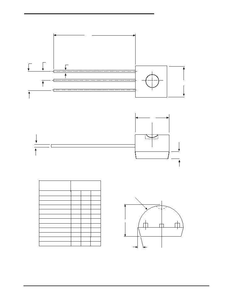
DIMENSIONS
IN
INCHES
3 PIN TO-92
A
b
E
e
e1
W
S1
R
L
.170
.016
.095
.105
SYMBOL
MIN NOM MAX
.014
-
.020
.195
.130
.045
.055
0.022
.175
4∫
.195
6∫
-
-
-
-
-
-
-
.500
.610
-
-
-
.085
.095
.045
.060
D
a
.155
3 PIN TO-92
PACKAGE: 3PIN TO-92
7
Date: 05/25/04 SPX2931 100mA Low Dropout Voltage Regulator
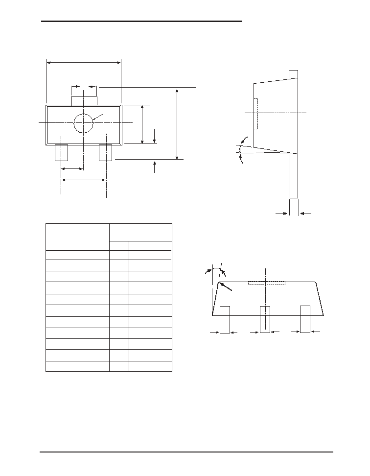
© Copyright 2004 Sipex Corporation
H
E
e
e1
D
D1
1
2
3
1.40 1.50 1.60
Dimensions in (mm)
3 PIN SOT-89
0.36 0.42 0.48
4.40 4.50 4.60
A
b1
C
D
H
E
L
MIN NOM MAX
1.40 1.60 1.75
3.94 - 4.25
e
e1
ÿ1.0
C
5∫(2x)
b
b1
b
Ro.15
8∫(2x)
b
0.41 0.47 0.53
0.38 0.40 0.43
D1
1.45 1.50 1.55
2.90 3.00 3.10
2.40 2.50 2.60
0.80 - 1.20
L
3 PIN SOT-89
PACKAGE: 3PIN SOT-89

8
Date: 05/25/04 SPX2931 100mA Low Dropout Voltage Regulator
© Copyright 2004 Sipex Corporation
Corporation
ANALOG EXCELLENCE
Sipex Corporation reserves the right to make changes to any products described herein. Sipex does not assume any liability arising out of the
application or use of any product or circuit described herein; neither does it convey any license under its patent rights nor the rights of others.
Sipex Corporation
Headquarters and
Sales Office
233 South Hillview Drive
Milpitas, CA 95035
TEL: (408) 934-7500
FAX: (408) 935-7600
ORDERING INFORMATION
PART NUMBER
ACC.
OUTPUT VOLTAGE
PACKAGE
SPX2931AM1-3.3
2%
3.3V
3 lead SOT-89
SPX2931AM1-3.3/TR
2%
3.3V
3 lead SOT-89
SPX2931AM1-3.5
2%
3.5V
3 lead SOT-89
SPX2931AM1-3.5/TR
2%
3.5V
3 lead SOT-89
SPX2931AN-3.3
2%
3.3V
3 lead TO-92
SPX2931AN-3.3/TR
2%
3.3V
3 lead TO-92
SPX2931AN-3.5
2%
3.5V
3 lead TO-92
SPX2931AN-3.5/TR
2%
3.5V
3 lead TO-92
SPX2931M1-3.3
3%
3.3V
3 Lead SOT-89
SPX2931M1-3.3/TR
3%
3.3V
3 Lead SOT-89
SPX2931M1-3.5
3%
3.5V
3 Lead SOT-89
SPX2931M1-3.5/TR
3%
3.5V
3 Lead SOT-89
SPX2931N-3.3
3%
3.3V
3 Lead TO-92
SPX2931N-3.3/TR
3%
3.3V
3 Lead TO-92
SPX2931N-3.5
3%
3.5V
3 Lead TO-92
SPX2931N-3.5/TR
3%
3.5V
3 Lead TO-92
Available in lead free packaging. To order add "-L" suffix to part number.
Example: SPX2931AN-3.3/TR = standard; SPX2931AN-L-3.3/TR = lead free
/TR = Tape and Reel
Pack quantity is 2,000 for TO-92 and 2,500 for SOT-89.